Z80 notes
1. Z80 Notes
1.1. Project log
1.1.1.
The 20MHz Z80s showed up yesterday \o/, not that I have time to do anything with them yet. On the bus this morning, I laid out a clock module and CPU carrier board; the routing is pretty gnarly but I didn't want to spend the time hand routing everything for a dev board. I'm working on the memory board now, and hoping to get everything done and ordered by the end of the day.
Debating using an m328 as the I/O controller. That would give me a serial port, and I could use I2C for most of the peripherals.
Another realisation I had while reading the Teensy Z80 post is that I can simulate a clock using an Arduino, which would also let me manipulerate the other pins, too.
On the subject of the SREC parser and serialiser, I kind of had this pet dream of building one that works a character at a time (e.g. fed from the USART). That requires building out the state machine (which I should probably draw out) and probably adding some callback functions once a record is ready.
1.1.2.
I started writing an SREC implementation in C++ that would work on an Arduino. I'm calling it the AEPRO - Arduino EEPROM programmer. I had been thinking I would just do write-only, but it would be almost criminal to not be able to verify that the EEPROM was written correctly. That led to poking around for a PISO equivalent of the 74595, which led to finding the MCP23008. That's an I2C I/O expander; three of them still only requires two pins on the Arduino and there's fewer chips on the board than with a SIPO/PISO combination and I get full I/O on the data pins. So I got that laid out right quick and ordered.
1.1.3.
I think the next steps for the Z80 project are twofold:
First, I need an EEPROM programmer. Right now I don't have a way to upload programs to the EEPROM, and that should not be so. I have a handful of SN74HCT595s, so I'll probably slap those on an Arduino and call that particular cat skinned, at least for a first pass at programmer. Following that, I'd like to make a ZIF-socket shield and figure out how to read data from the EEPROM. I envision that this is a serial interface for maximum justice or whatever.
The second thing is I need an EEPROM to program; to wit, I need a way to connect the two boards together. Now this turns out to be more of a challenge than I thought previously for a number of reasons:
- My EDA software (Eagle) is limited in the number of layers (maximum of two), sheets (2), and board size (eurocard).
- I am unwilling to pay $100/year for a subscription-only upgrade when I paid $160 for a fully unlocked version several years ago.
- The alternative EDA software, Kicad [1], is pretty bad. I can symapthise with the plight of open source software, but I can't use it. So far, every attempt at learning it has lasted about 15 minutes before I have to go to Eagle to get done what I set out to do. I'll keep trying, but this is kind of like training yourself to enjoy surströmming.
- It turns out to be hard to layout everything in one schematic, and a Eurocard-sized board isn't really big enough.
One idea I've been floating around is using IDC40 cables (e.g. the same connector used on ATA drives and the Raspberry Pi's GPIO header) which coincidentally have as many connections as the Z80 has pins. This would let me build small boards, like a CPU board and separate clock boards, without having to commit to an overall board design early on. It also lets me vet components in stages - first I can make test the clock, power, and basic Z80 functionality; then, I can check the memory subsystem, etc.
To that end, I think it'd be useful to have a jumper on the clock line so that I can also inject an external clock in order to use a manual timing cycle.
Another idea was stacking boards using the same sort of connector, similar to how the raspberry pi does its add-on boards.
1.1.4.
Lots of designing today. Some thoughts:
It would be cool to have an ESP8266-based modem; send a connect command (SSID and password), then another connect command to set host and port. The terminology for this needs to be sorted out. I was thinking of a gopher browser and an IRC client.
Graphics remains an open question, and there's two main questions. The first is what chipset to use, the second is how to deal with the VRAM requirements.
For graphics chipsets, there are a number of options that I see with more to come later as I do more research. The SSD1306 is a venerable chipset, but I don't really like the dimensions - all of mine are extremely small displays with 128x64 or 64x64 pixels. I'd like at least 5.7", with 7" closer to my ideal. Another option that I've seen is the KS018 chipset - I've never used it, but keeping it in mind.
There's also the option of using an AVR as a GPU, which might help with the VRAM issue, which is essentially that, at 320x240 pixels, requires tracking 75k of pixels. If I do this as a bitmap (each byte representing 1 pixel), then that's still roughly 9.5k of memory. I could put another RAM chip on the I/O bus and hook it up as VRAM, maybe? Not really sure.
I wonder if it might be easier to implement an interface that's text-only; rather than drawing pixels, the Z80 sends the characters to print. I'm really just not sure yet.
I also did a writeup on the memory layout, which is in the design section.
1.1.5.
Watching HCF made me want to build my own computer, and of course, it should be a laptop. My first inclination was a 6502-based system, but I just got the RC2014 which is made me think I should do a Z80. Then, I found Steve Ciarcia's "Build Your Own Z80 Computer" and I guess that's that. I have no idea what I'm doing here, so I expect to learn a lot.
I'm thinking a 7" display, some kind of mechanical keyboard. The first iteration probably won't do sound for simplicity's sake. For the power supply, I was thinking micro USB or USB-C to an internal LiPo pack, but I think I might just do a pair of 18650s. The first revision probably won't have a charging circuit inside; I might do a barrel jack connector too, but will need make sure to disable the battery if it's powered that way.
1.2. Design
1.2.1. Memory layout
While trying to figure out how to add memory and EEPROM to the machine, I had a hard time finding good information on how to do this; even harder was finding a writeup of the thought process behind this. So, as best as I understand it, here's how you add memory to the Z80.
While the Z80 is an 8-bit processor, it has a 16-bit address space (address pins A0…A15), which means it has a maximum of 65,535 bytes (64K) of accessible memory. This address space has to be split between ROM and RAM (fortunately I/O devices have another access mechanism). The task is to figure out what the split should be and how to accomplish it.
In the case of my computer, I'm using an AT28C256 32KB parallel
EEPROM with a CY62256 parallel SRAM chip; because the CY62256 is
32KB, we need two of them to get the full address space. All three
of these pins have a chip enable pin /CE; the leading slash in
front of the pin name indicates active-low logic. With active high
signalling, a high signal (i.e. a digital 1 or +5V) means active,
but with active low signalling, a LOW signal means
active. Basically, when /CE is pulled to ground, the chip is
enabled. Note that the chips have slightly different names for
these pins but they have the same function. For consistency, I'll
just use one set of names.
It's important to know that the Z80 starts execution at address
0000H, which implies that the ROM should occupy the bottom of
the address space. In that case, if we look at the binary
representation of addresses, we can make some observations that
will govern how we lay out memory:
MSB            LSB
  111111
  5432109876543210
+------------------+-------+
| 0010000000000000 | 8192  |
| 0100000000000000 | 16384 |
| 1000000000000000 | 32768 |
+------------------+-------+
If we give 8K of space to the ROM, we get 56K of RAM and an easy
way to tell which chip should be selected: address pins A13,
A14, and A15 decide which of our three chips should be
chosen. The selection table looks like this:
| A13 | A14 | A15 | chip |
|---|---|---|---|
| L | L | L | ROM |
| x | x | H | RAM1 |
| L | x | L | RAM0 |
| x | L | L | RAM0 |
Basically, the three conditions are:
- the ROM should be chosen if
NAND(A13, A14, A15). - RAM1 should be chosen if
A15 - RAM2 should be chosen if
AND(NOT(A15), OR(A13, A14)).
This could be done with logic gates, though it might get a
little messy on the board. Fortunately, there's a 7400 series
chip that does a lot of heavy lifting for us: the 74139 (I'm
using the TI SN74HCT family, e.g. the SN74HCT139) 2-of-4 decoder
and demux. It has three input pins (/E, A0, and A1) and
four output pins (O0, O1, O2, O3). The enable pin is
active low while the address pins are active high, so this can be
a little confusing, but let's figure this out. Here's the 74139's
logic table where H means HIGH and L means LOW (as in signal
levels); I've added a final column that expresses the output pins
as a binary value with O0 as the LSB. Note that if /E is low,
it doesn't matter what A0 and A1 are - the output will be all
high values.
| /E | A0 | A1 | O0 | O1 | O2 | O3 | O |
|---|---|---|---|---|---|---|---|
| H | x | x | H | H | H | H | 1111 |
| L | L | L | L | H | H | H | 1110 |
| L | H | L | H | L | H | H | 1101 |
| L | L | H | H | H | L | H | 1011 |
| L | H | H | H | H | H | L | 0111 |
There's an important property of this chip: at most one output
pin is low. If it's not enabled (e.g. /E is high), then none of
the output pins are low. This is what we want when using active
low logic to select a memory chip. At most one device is active,
and if disabled, no devices are active.
The Z80 indicates that the address bus has a memory address by
pulling its /MREQ pin low; we'll tie that to the /E pin. We
can put pins A13 and A14 into a 7432 OR gate, and connect
that to A0. Note that you should connect the unused gate pins
to ground. A15 gets connected to A1, which means we can
revise our table (condensing the output pins to a single binary
value for clarity).
| /MREQ | A13 | A14 | A0 | A15 | O | Notes |
|---|---|---|---|---|---|---|
| H | x | x | x | x | 1111 | no memory operation |
| L | L | L | L | L | 1110 | address is < 8192 |
| L | H | L | H | L | 1101 | |
| L | L | H | H | L | 1101 | |
| L | H | H | H | L | 1101 | |
| L | x | x | L | H | 1011 | if A15 is high, it doesn't really matter what A0 is. |
| L | x | x | H | H | 0111 |
So far, we know we can tie O0 directly to the ROM's /CE pin,
and O1 directly to RAM1's /CE pin. But how do we combine O2
and O3? Let's see what we want, behaviour wise.
| O2 | O3 | /CE | Notes |
|---|---|---|---|
| H | H | H | if both pins are high, /CE should be high. |
| L | H | L | if either O2 or O3 are low, /CE should |
| H | L | L | be low. |
This looks almost like an AND gate, which would also pull /CE
low if both O2 and O3 are selected. There isn't a case where
this happens, so we don't need to consider it. That means we
should tie O2 and O3 together behind a 7408 AND gate. Lets
simplify the table above, with A0=OR(A13,A14) and
O=(AND(O2,O3),O1,O0).
| /MREQ | A0 | A15 | O | Memory device |
|---|---|---|---|---|
| 1 | x | x | 111 | None |
| 0 | 0 | 0 | 110 | ROM |
| 0 | 1 | 0 | 101 | RAM0 |
| 0 | x | 1 | 011 | RAM1 |
But does this actually work? Let's verify the basic idea in Python. First, let's write a function that returns the memory chip for a given three-bit value:
def chip_selected(pins):
    if pins == 0b111:
        return None
    elif pins == 0b110:
        return "ROM"
    elif pins == 0b101:
        return "RAM0"
    elif pins == 0b011:
        return "RAM1"

    raise Exception("multiple devices active ({})".format(bin(pins)))
Now, let's emulate the 74139:
def demux(e, a0, a1):
    if e:
        return (1, 1, 1, 1)
    if a1:
        if a0:
            return (1, 1, 1, 0)
        return (1, 1, 0, 1)
    if a0:
        return (1, 0, 1, 1)
    return (0, 1, 1, 1)
This is really just hardcoding the logic table above. Okay, now the meat of the problem: actually checking our addresses:
def memselect(mreq, addr):
        # ex. memselect(0, 0x8000)
    # mreq is active high, so it should be 0 or False to enable
    # memory devices.

    # the address bus is 16 bits
    addr = addr & 0xFFFF

        # get our three chip selection bits from the address.
    a13 = addr & (1 << 13)
    a14 = addr & (1 << 14)
    a15 = addr & (1 << 15)

    # select an address.
    a0 = a13 | a14
    a1 = a15
    (o0, o1, o2, o3) = demux(mreq, a0, a1)
    ando = o2 & o3
    muxval = (ando << 2) | (o1 << 1) | o0

    return chip_selected(muxval)
Now we should be able to write a self test for this; there's few enough memory addresses that we can test all of them.
def self_test():
    """test all 16-bit addresses against their expected memory chip."""

    for addr in range(0, 8192):
        assert memselect(0, addr) == "ROM"
        assert memselect(1, addr) == None
    print("ROM: OK")

    for addr in range(8192, 32768):
        assert memselect(0, addr) == "RAM0"
        assert memselect(1, addr) == None
    print("RAM0: OK")

    for addr in range(32768, 65536):
        assert memselect(0, addr) == "RAM1"
        assert memselect(1, addr) == None
    print("RAM1: OK")
Hey, look at that - it works!
The memory chips also have a write enable pin, /WE, and an
'output enable' pin, /OE. These tell the chip whether a read or
write is occurring. For the ROM, it might make sense not to wire
in the write enable line, tying it to ground instead to hardwire
a write protect. Either way, you can attach the Z80's /WR pin
to all three pins /WE and the /RD pin to all three's /OE
pin. Throw in some power and you got yourself a memory bus. Total
parts list (apart from the Z80), with digikey part numbers:
| Qty | Part | Digikey Part |
|---|---|---|
| 1 | AT28C256 | AT28C256-15PU-ND |
| 2 | CY62256 | 1450-1480-ND |
| 1 | SN74HC139 | 296-8230-5-ND |
| 1 | SN74HC08N | 296-1570-5-ND |
| 1 | SN74HC32N | 296-1589-5-ND |
Here's a schematic of this, with just enough wiring to show the layout:
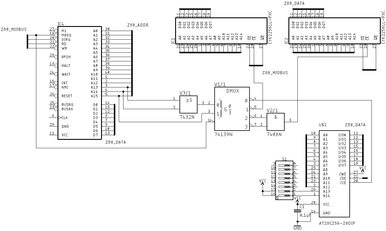
Finally, there are some things to note: the Z80's pins should
still be buffered, which is something for a later post. This also
isn't the most efficient use of the space available, as there's
an 8K hole that's never used in RAM0's address space and we're
also only using a quarter of our ROM space. If we wanted to
support multiple 8K ROMs, we could add a DIP-2 switch to address
pins A13 and A14 on the EEPROM. Basically:
| A13 | A14 | EEPROM address | ROM |
|---|---|---|---|
| 0 | 0 | 0-1FFFH | 0 |
| 1 | 0 | 2000H-3FFFH | 1 |
| 0 | 1 | 4000H-5FFFH | 2 |
| 1 | 1 | 6000H-7FFFH | 3 |
Just a thought.
1.3. Related links
1.3.1. Z80 computers
1.3.2. Memory management
- Retro Z80: Deciding on Memory Design
- Z80 memory space
- Wiring a Z80 - interesting note: "a proper Z80 based design should buffer all output pins"